


Rs 162 only/-
9907385555 asingh039@gmail.com
MP NAGAR BHOPAL
The continuous demand of portable battery bank operated high speed microprocessor based portable devices like smart phone, notebook, mini laptop computers, etc. increase every day. High speed portable devices integrated with primary memory that responds faster. The circuit with high value of VDD offers higher operating speed (less delay) at a cost of high power dissipation. While, as we decrease the VDD, the circuit design offers lower operating speed (high delay) at a cost of low power dissipation. To vary the supply voltage at various method of operation Power-on-Reset circuit is utilized.
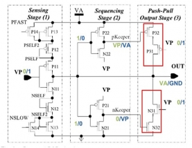
We designed and implemented the novel modified POR circuit using forced stack topology in the 45-nm CMOS technology using 16 Transistor. We used silicon qualified SPICE models to simulate the netlist along with parasitics, at extended corner lot points of the process for nMOS (N) and pMOS (P) temperature 25 °C and VDD=1Volt sing HSPICE EDA Tool. POR can be characterized on the basis of following parameters such as wake-up time, power dissipation, Energy and Transistor count. The proposed technique is compared with the new existing technique POR-LE. The proposed design is based on stacking of pull-up and pull-down transistor in push-pull output stage also called sleepy approach to reduce the energy consumption of POR circuit.


| Doc | Complete Project word file document |
