Project Discription
05-October-2018
When used as an AC signal amplifier, the transistors Base biasing voltage is applied in such a way that it always operates within its “active” region, that is the linear part of the output characteristics curves are used.
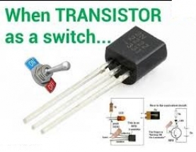
The circuit resembles that of the Common Emitter circuit we looked at in the previous tutorials. The difference this time is that to operate the transistor as a switch the transistor needs to be turned either fully “OFF” (cut-off) or fully “ON” (saturated). An ideal transistor switch would have infinite circuit resistance between the Collector and Emitter when turned “fully-OFF” resulting in zero current flowing through it and zero resistance between the Collector and Emitter when turned “fully-ON”, resulting in the maximum current flow.
In practice when the transistor is turned “OFF”, small leakage currents flow through the transistor and when fully “ON” the device has a low resistance value causing a small saturation voltage ( VCE ) across it. Even though the transistor is not a perfect switch, in both the cut-off and saturation regions the power dissipated by the transistor is at its minimum.
In order for the Base current to flow, the Base input terminal must be made more positive than the Emitter by increasing it above the 0.7 volts needed for a silicon device. By varying this Base-Emitter voltage VBE, the Base current is also altered and which in turn controls the amount of Collector current flowing through the transistor as previously discussed.
When maximum Collector current flows the transistor is said to be Saturated. The value of the Base resistor determines how much input voltage is required and corresponding Base current to switch the transistor fully “ON”
Other Detail
Software Requirement :
No
Hardware Requirement : NPN transitor